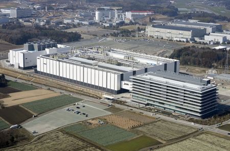

Taiwan Semiconductor Manufacturing Company, the globe’s leading contract semiconductor producer, will begin equipment setup and full-scale manufacturing of ultra-advanced 3-nanometer wafers by 2028 at its second Japanese manufacturing facility, according to a Tuesday evening government document filed in Taiwan.
During a February meeting with Japan’s Prime Minister Sanae Takaichi, TSMC Chief Executive CC Wei announced the company’s intention to begin large-scale production of state-of-the-art 3-nanometer semiconductors at the second Japanese manufacturing site.
The updated blueprint calls for the second Japanese chip manufacturing facility to produce 15,000 12-inch wafers each month using cutting-edge 3-nanometer processing methods, Tuesday’s filing revealed.
This represents a significant shift from TSMC’s earlier Japanese operations, which concentrated on older semiconductor technologies. The company announced in 2024 that combined investment in both Japanese facilities would surpass $20 billion, with total monthly output reaching 100,000 12-inch wafers using older 40, 22/28, 12/16 and 6/7-nanometer processes.
Japan’s Yomiuri newspaper reported in February that the second facility’s investment would approach $17 billion, though TSMC has not confirmed this amount and refused to comment on the reported spending figure.
TSMC’s initial Japanese manufacturing plant began high-volume production in late 2024.
The semiconductor giant created its Japanese division, Japan Advanced Semiconductor Manufacturing, in 2021 with backing from Sony Semiconductor Solutions Corporation. DENSO Corporation and Toyota Motor Corporation subsequently became minority stakeholders in the venture.