
A Dutch technology firm has reached a major breakthrough in semiconductor manufacturing, announcing that their revolutionary chip-making equipment is now ready for widespread industrial use.
ASML Holding, the Netherlands-based company that manufactures the world’s only commercial extreme ultraviolet lithography equipment, revealed Wednesday that their latest generation machines have achieved the performance standards necessary for mass production operations.
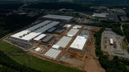
These advanced manufacturing systems will enable major chip producers like Taiwan Semiconductor Manufacturing and Intel to create more sophisticated and energy-efficient processors while streamlining their production methods, according to company data.
Marco Pieters, ASML’s chief technology officer, shared this milestone information with Reuters ahead of a technical presentation scheduled for Thursday in San Jose, California.
“I think that it’s at a critical point to look at the amount of learning cycles that have happened,” Pieters explained, discussing the extensive testing customers have performed on these machines.
The development comes at a crucial time as current chip-making technology approaches its technical boundaries for producing complex artificial intelligence processors. These new High-NA EUV systems are essential for advancing AI applications like OpenAI’s ChatGPT and helping semiconductor companies meet growing market demands.
Each of these cutting-edge machines carries a price tag of approximately $400 million, double the cost of previous-generation equipment.
According to Pieters, the High-NA EUV systems have demonstrated their reliability by maintaining minimal downtime, processing 500,000 dinner-plate-sized silicon wafers, and achieving the precision needed to create intricate circuit patterns. These three performance indicators collectively demonstrate the equipment’s readiness for manufacturing use.
“(Chipmakers) have all the knowledge to qualify these tools,” Pieters stated.
However, despite their technical capabilities, manufacturers will need an additional two to three years to complete sufficient testing and development work before fully incorporating these systems into their production lines.
The company has currently achieved approximately 80% uptime with their equipment and aims to reach 90% efficiency by year’s end. Pieters noted that the imaging capabilities they plan to showcase will demonstrate how a single High-NA process can replace multiple steps required by older technology. The half-million wafers processed have allowed engineers to resolve numerous operational challenges.